Columbia University and Brookhaven National Laboratory researchers have unveiled a groundbreaking method to engineer intricate three‑dimensional nanostructures entirely through DNA self‑assembly in aqueous environments. This technique, underpinned by an innovative algorithm called MOSES, promises to shift current paradigms in nanomanufacturing, with potential applications in optical computing, neuromorphic hardware, biotechnology and beyond.
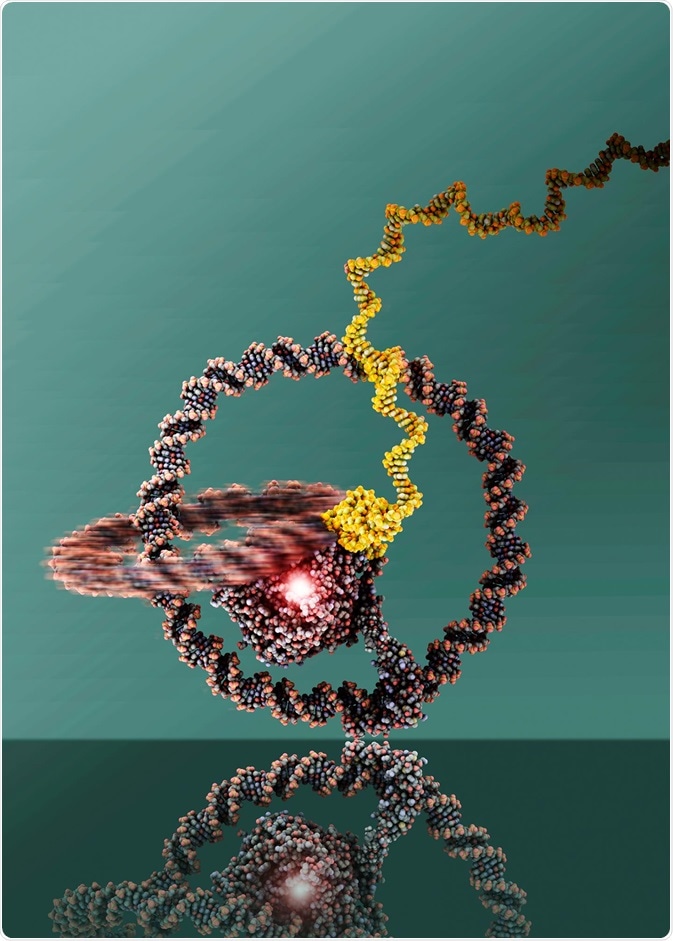
At the heart of this advance are DNA‑based “voxels”—octahedral units formed by folding DNA strands into robust polyhedral shapes. Each voxel carries programmable connectors at its vertices, enabling predictable binding to other voxels. The MOSES algorithm orchestrates these voxels into prescribed motifs and assembles multiple motifs in parallel, all within a single solution, creating hierarchically organised nanostructures.
By replacing conventional top‑down fabrication techniques such as photolithography—which etch material layer by layer—or additive manufacturing, which cannot operate at the nanoscale, this bottom‑up, water‑borne method expedites production and broadens design capabilities. The process was described in new research published 9 July in Nature Materials, following earlier complementary work in ACS Nano.
Oleg Gang, professor of chemical engineering at Columbia and leader of the Soft and Bio Nanomaterials Group at Brookhaven’s Center for Functional Nanomaterials, described the technique as akin to constructing a nano‑scale Empire State Building: “We can build now the complexly prescribed 3D organisations from self‑assembled nanocomponents”.
The research demonstrates MOSES’s versatility through multiple showcase structures. These include crystal‑like lattices of one‑dimensional strings, two‑dimensional layers, helical swirls and reflective arrays, with potential relevance to neuromorphic computing, catalytic systems and optical computing architectures.
Detailed molecular insights emerged from a parallel study at Brookhaven, which featured the transformation of DNA‑nanoparticle lattices into silica‑reinforced replicas. These maintained structural fidelity while gaining resilience, enduring extreme conditions such as temperatures above 1,000 °C and pressures exceeding 8 GPa. Brookhaven‑led experiments also employed X‑ray computed tomography at 7 nm resolution to examine internal structure, verifying precise assembly and mapping defects.
This hybridisation of DNA‑templated self‑assembly with known inorganic material procedures means that the resulting structures can maintain functionality in demanding environments and are compatible with customary lithographic processes. Such convergence significantly lowers the barrier to integrating DNA‑assembled nanomaterials into mainstream microelectronic workflows.
Academic commentary underscores the novelty of the MOSES‑driven inverse design strategy, which streamlines lattice generation by pairing symmetry considerations with minimised voxel libraries, reducing complexity while ensuring precise assembly. The strategy adeptly adapts to a variety of lattice symmetries, including zinc blende and cubic Laves phases, as well as custom motifs.
This strategy builds upon decades of DNA nanotechnology foundations—initiated by Nadrian Seeman’s early work in the 1980s—and refined through Paul Rothemund’s introduction of DNA origami in 2006. The current advance marks a decisive shift: forcing DNA frameworks out of purely biological or soft matter domains into the realm of durable, engineered materials.
Existing challenges include scalability and assembly yield. Coating DNA structures with silica requires precise control to obtain uniform layers, and as structures ascend in complexity, error‑reduction becomes critical. Additionally, integrating inorganic components like metals or semiconducting nanoparticles introduces new binding and compatibility challenges. Yet the modular voxel‑based assembly approach is well suited to iterative error correction, and continued work on interface chemistry aims to improve yield and robustness.
The marketplace potential spans diverse sectors. In optical computing, reflective lattice architectures could form nanoscale waveguides or mirror arrays. Neuromorphic systems may benefit from DNA‑templated catalytic networks or sensor arrays. In biotechnology, bio‑scaffolds constructed with programmable porosity could revolutionise tissue engineering and drug delivery.
With funding from the US Department of Energy’s Office of Science and broader support through initiatives like the National Nanotechnology Initiative, the field is experiencing accelerated development. Columbia and Brookhaven’s contributions spearhead a wave of innovation in programmable nanomaterials, suggesting that bottom‑up design may soon rival or surpass traditional top‑down processes at ever‑smaller scales.